Why Advanced Packaging Materials Matter?(Part B)

Editor’s Note: “Tech Forum” is a new section of our English website. It will feature in-depth technical articles instead of news reporting by our analysts and guest experts in China’s mainland and around the world including the Taiwan region. Our first article, “Why Advanced Packaging Materials Matter?” gives insights in two parts on this new frontier of semiconductor technology developments. Following is the Part B of the article.
iii. Organic Substrate
High volume usage of organic substrates started in the 1990s. Driven by ceramic package’s high costs and electric performance limitations, Intel moved to an organic laminate-based Plastic Pin Grid Array(PPGA) package for its Pentium processors. Motorola extended the flip chip concept to carrier level and popularized Plastic Ball Grid Array (PBGA) package. For DRAM memory packaging, a CSP (Chip Scale Package) type of window BGA, gained market share over the conventional leadframe based TSOP package by delivering advantages in packages size and electrical performance. A main driver for this conversion was the commercialization of BT laminate. BT resin was developed by Mitsubishi-Gas Co. to replace the standard FR-4 epoxy resin for high-end circuit boards. BT-epoxy formulations, having Tg around 180ºC, were used for substrate production in volume. Availability of low temperature solder bump and underfill resin opened an application space for flip chip attachment. It is also a suitable carrier base for ABF (Ajinomoto Build-up Film) build up layers. Substrate having BT laminate and ABF layers are now the main stay for high performance packaging. A more detailed discussion follows.
A condensation type of polyimide based on PMDA-ODA (pyromellitic anhydride-oxydianaline) was the first high temperature resistant polymer widely used in the electronic industry. It is a versatile dielectric material which can be spin coated for thin film processing or formed a tape for use as chip carrier.
TAB (Tape Automatic Bonding) is a packaging type using polymer tape as chip carrier and processed by roll-line manufacturing. Electrical connections are achieved by attaching cantilever beam leads to the chip bonding pads. Chip-on-film (COF) accommodates a fine pitch flip chip attachment to a polyimide tape carrier. Upilex®, a structurally rigid lower CTE polyimide tape, is being used in volume production as substrate for display drivers. The smart card industry uses “microconnectors” fabricated by polyimide tape as substrate. It is estimated that close to 10 billion smart cards were shipped in 2021. Currently there are about 30 to 50 billion smart cards of various types, such SIM and bank cards, in circulation today.
Many technology attributes derived from various innovations we mentioned above have become key enablers to the recent development of high-performance packaging, which includes, PoP, heterogeneous integration (HI), 2.5D, 3D, TSV, WLCSP, etc.
c. Advanced Packaging-Heterogeneous Integration/Chiplets
Affected by the high production costs of new technology nodes and expected process yield losses, the economics of a semiconductor unit has started plateauing and adding a premium on a monolithic large chip when compared to previous generation products. As this Moore’s Law of scaling is getting more expensive, advanced packaging is being leveraged to deliver monolithic SoC’s (System-on-Chip) functionalities by chiplet packages, in which smaller dies (chiplets) each provide part of the SoC functional region are connected using packaging level integration.
This trend is illustrated by an example that estimates Apple SoC’s scaling efficiency is diminishing (Table 4) while fab capex investment continues to rise (Figure 4). To overcome the anticipated silicon scaling limitation, extensive development work commenced in the early 2000s using packaging solutions for chiplet connections to match a monolithic chip’s functionalities. As a result, a new “mid-end” segment has gained a lot of the attention using Heterogeneous Integration (HI) solutions to meet the continuous demand for improved system performance. This segment of work involves integrating many front-end and back-end technologies for an application space between the two (Figure 5).

Table 4. Apple monolithic SOC transistor scaling / SemiAnalysis
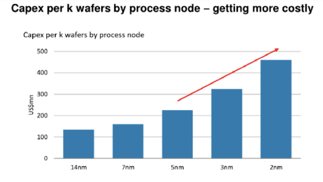
Figure 4. Fab capex vs technology node / Morgan Stanley
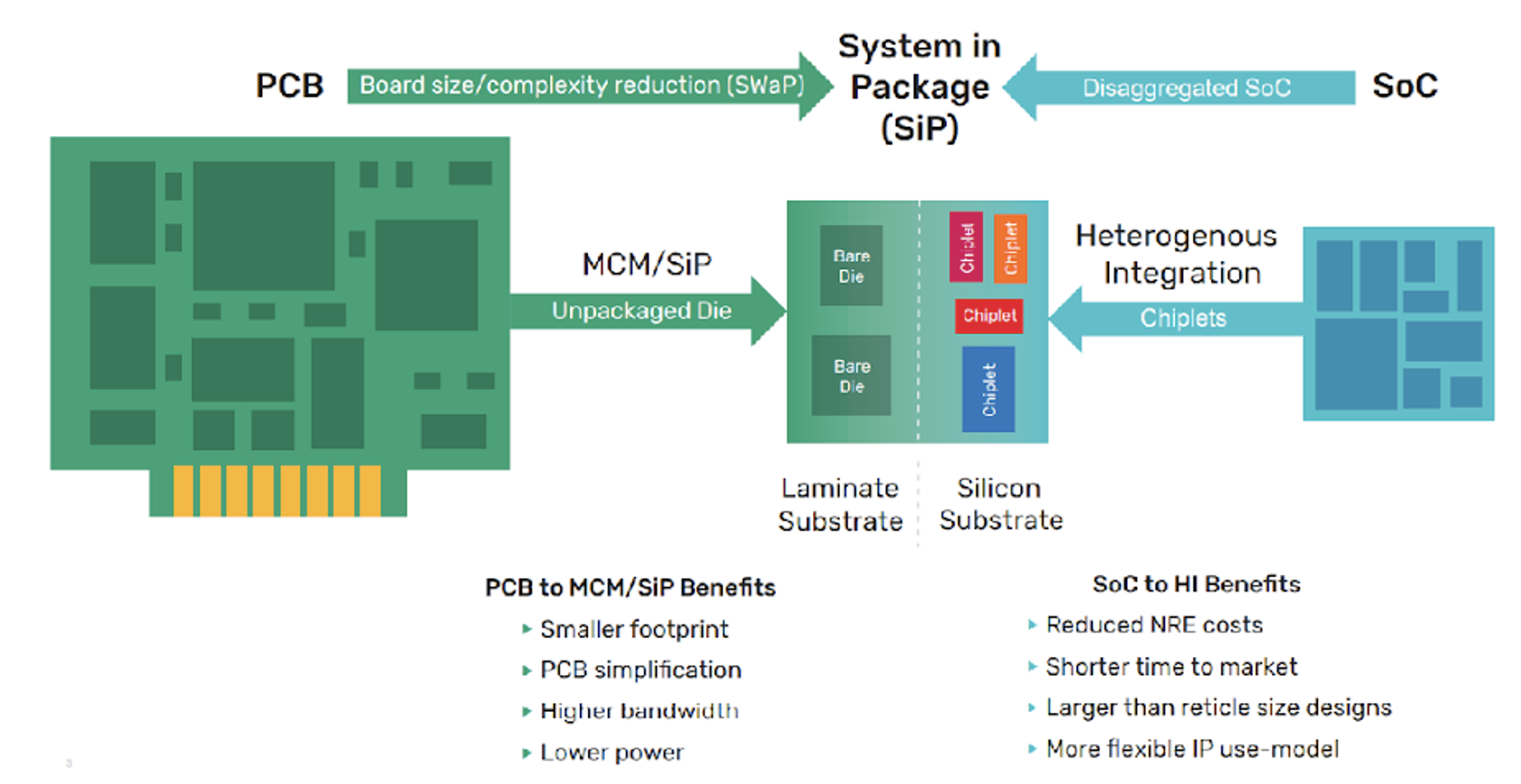
Figure 5 /Cadence
Many materials for packaging have been developed for use in high performance and mobile applications, such as:
-Use of build-up RDL on either organic or silicon substrates for 2.5D integration
-TSV formation and 3D stacking for active devices or for interconnects on passive silicon carrier
-Fine pitch wring
-New area array bumping metallurgy and bonding processes
Heterogeneous integration leverages advanced packaging techniques to integrate various components, that also can be in mixed nodes, into a package to match the functionality and performance of a monolithic SoC or in a form of SiP. The key attributes of three types of products in high volume manufacturing are discussed below.
Xilinx Virtrx-7 7000
The first commercial usage of TSV technology for high density packaging was in 2011 by Xilinx and TSMC Instead of building a large monolithic chip, Vitrex-7 adopted a package level solution to interconnect four 28nm dies onto a 2.5D TSV interposer. Figure 6 illustrates the use of 100um thick silicon interposer having 10um TSVs and 45-micron pitch microbumps. The assembly of interposer to a 4-2-4 BT/ABF BGA substrate was achieved by flip chip bumps at 180um pitch. This structure illustrates the use of TSMC CoWoS (Chip-on-Wafer-on-Substrate) approach.
This was an example that a high-performance product could be enabled by dense die-to-die connections in the package. New innovations combined with proven packaging processes have successfully furthered the usage of silicon interposer technology in advanced packaging.
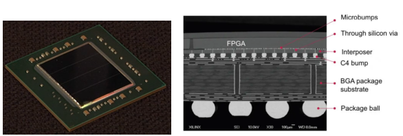
Figure 6. Xilinx Virtrx-7 Package / Xilinx (Left) ;SemiWiki (Right)
Intel EMIB Core i7
Intel introduced its Kaby Lake Gprocessor (Figure 7) to the consumer market in 2017. The processor package contains a CPU, a graphics processor (GPU) from AMD and a high bandwidth memory (HBM2) from Samsung, in which Embedded Multi-die Interconnect Bridge (EMIB) technology was used to interconnect adjacent GPU and HBM2 memory. EMIB is a variant of 2.5D technology. Development work started in the 2000s with an aim to provide a flexible interconnection method which can be readily tailored to meet different I/Os and functionality requirements.
As illustrated in figure 7 that GPU and HBM2 memory are connected by a piece of silicon. There are four build-up Cu wirings (2um line/2um space) on top of a small bridge die. It is then placed in a laminate cavity followed with dielectric layer lamination/encapsulation and top layer bond pad circuitry formation to complete the embedding of silicon bridge die into substrate (Figure 8). A Standard assembly process is used for flip chip attachment. Dual Cu pillar bump pitches present on active silicon die (Figure 9). For chip-to-bridge die connections, microbumps used are at 55um pitch.
The EMIB is built upon an extension of existing organic laminate structure. High bandwidths die-to-die edge connections are achieved by densely wired passive interposer without TSVs. As this organic substrate technology is further scalable to larger panel size the opportunities for further savings are anticipated.
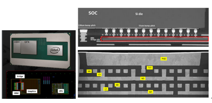
Figure 7. Intel EMIB Kaby Lake G Core i7 / Intel
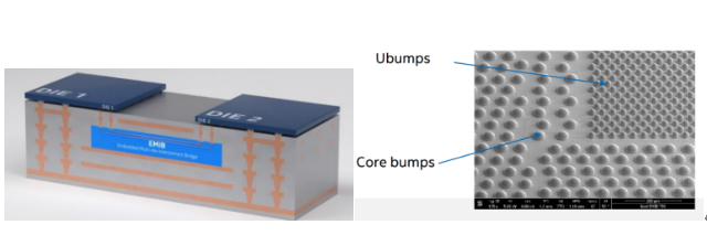
Figure 8. Intel Embedded bridge die / Intel Figure 9. Dual bump pitches / Intel
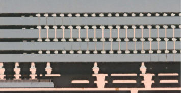
Figure 10. HBM2 connection to EMIB die / System Plus Consulting
AMD Radeon Vega GPU
As discussed above, in Intel’s Kaby Lake G module, AMD’s GPU and Samsung’s HBM2 memory were connected by a bridge die using EMIB technology. Around the same period, AMD also introduced the Vega GPU under its own brand featuring the integration of a GPU die with two 8G HBM2s in the package (Figure 11). This 2.5D assembly was built upon a TSV middle silicon interposer. The HBM2 3DIC memory consists of one controller die and 8 vertically stacked DRAM dies connected by microbumps and TSVs. A standard flip chip process is used for silicon interposer and substrate connection.
This is a good illustration that GPU+HBM memory integration achieved by both EMIB and TSV middle silicon interposer at packaging level. Figure 12 demonstrates the structural differences between the two. The use of a full-size silicon interposer consumes more material and is processed by front-end fab technologies, whereas the use of smaller EMIB bridge die is a more back-end-centric approach.
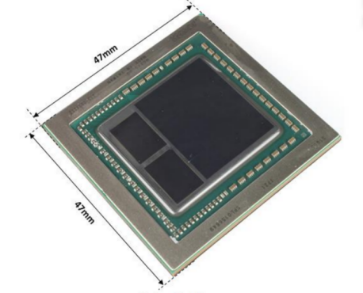
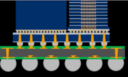
Figure 11. AMD Radeon Vega GPU / System Plus Consulting

Figure 12. Comparison of two types of silicon interposers / Intel
High density interconnections are achieved by the use of 2.5D silicon interposers that differ in size and construction in many ways. The key attributes of the three types of packages discussed above are summarized in Table 5.

Table 5. Advanced Package Key Attributes Comparison
By applying the embedded bridge die concept, more variation in package structures also have been reported by IBM, SPIL and TSMC.(Figure13-15)
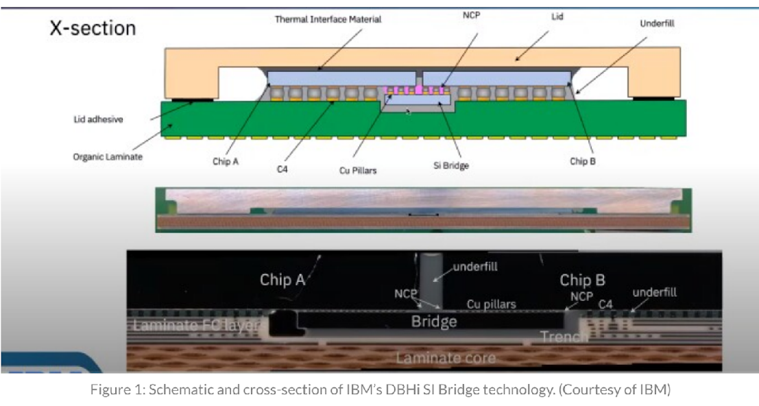
Figure 13. IBM’s DBNI silicon bridge packaging / IBM 3DIncites
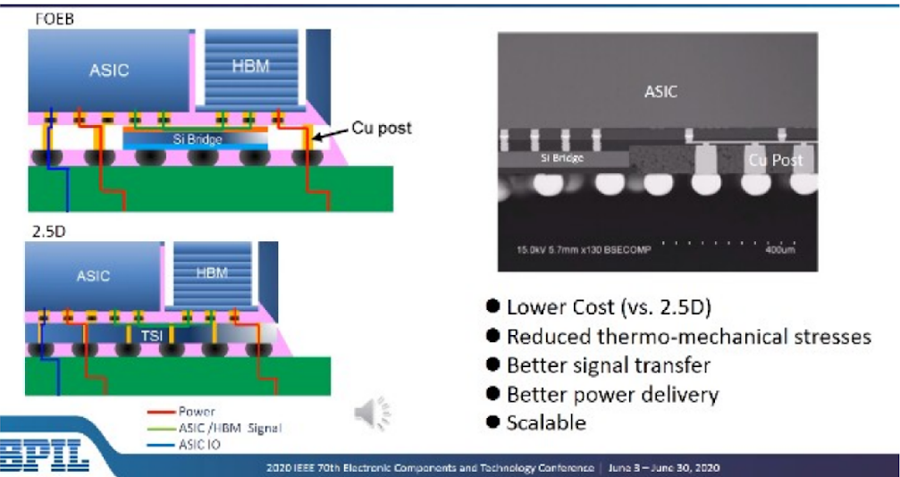
Figure 14. SPIL’s Fan Out Embedded Bridge (FOEB) package / SPIL
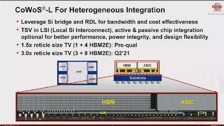
Figure 15. TSMC CoWoS with LSI (Local Silicon Interconnect) Bridge
The above examples illustrate that there are multiple ways to combine smaller dies with different functions by adopting advanced packaging processes. All six products use 2.5D silicon interposer for die-to-die interconnections, but their package structures are dissimilar. Unlike front-end processes that all happen on round wafers, back-end products come with vastly distinct types of factors and use specialized material sets. An engineer equipped with in-depth know-how can efficiently select matching materials and processes from the “toolbox” is essential to the success of delivering a competitive product. Driven by strong demand, two packaging materials, BT substrate and ABF film, received continued attention in the industry. We will discuss this in more detail in the follow-up sections.
Use of chiplet technology brings significant flexibility in the product architecture facilitated by the mixing of dies from several different sources. To accelerate this trend, a protocol may lower the barriers for achieving structured connectivity standard in the ecosystem. Recently, under Intel’s lead, ten companies, including AMD, ARM, TSMC, Microsoft, have jointly launched a chiplet standard alliance, the Universal Chiplet Interconnect Express (UCle), to address the issue. The aim is to have a single set of standard one can follow to simplify the design process and for ease of manufacturing. An open ecosystem is expected to accelerate the adoption of chiplet/heterogenous integration approach while packaging technology is now playing an increasingly critical role in achieving various cost and performance benchmarks of advanced electronics products.

*此内容为集微网原创,著作权归集微网所有,爱集微,爱原创

晶圆产能释放利好,溅射靶材三厂竞速


 专利申请
专利申请
 知识产权质押融资
 专利地图分析
 版权登记
版权登记
 集成电路布图设计
 商标交易
商标交易
 商标申请
商标申请
 专利交易
专利交易
 专利无效
专利无效


热门评论