Editing by Greg Gao
Dai Weimin, the founder and chairman of VeriSilicon, pointed out Chiplet – the new IP reuse technology - will be adopted in more advanced and highly integrated semiconductor devices in high-end laptop processors, autonomous driving, and data center.
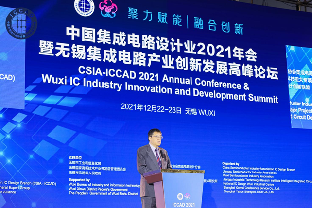
Dai delivered a keynote speech entitled "The Industrialization Road of Chiplet" at the annual conference of ICCAD, the top trade organization for China's IC design industry, on December 22. He said that Chiplet holds significant advantages in improved yield and cost-effectiveness, quick customization and meeting multiple functional requirements.
Dai founded VeriSilicon(芯原股份), a custom silicon services and semiconductor IP licensing services provider, in 2001 in Shanghai. According to media reports, the company is now the No.1 IP supplier in the Chinese mainland and seventh in the world.
Over the last couple of years, Dai has led his VeriSilicon team pioneering Chiplet technology in China. He proposed the concept of IP as a Chiplet (IaaC) and Chiplet as a Service. IaaC aims to achieve "plug-and-play" of special function IPs with Chiplet to strike a right balance between performance and cost in 7nm, 5nm, and more advanced processes, reducing the IC design time and risk.
In his speech, Dai said that the semiconductor industry faced several major bottlenecks in the post-Moore era, and it is getting urgent to resolve them. On the one hand, the design cost and complexity of advanced process chips have increased tremendously; On the other hand, the semiconductor market is getting more diversified, shortening the innovation cycle and boosting the demand for customized chips on the application side.
Chiplet has increasingly been regarded as the key technology to tackle the bottleneck with new chip architecture. The consultancy firm Omdia predicts that the global market size of Chiplet processors will increase from $645 million in 2018 to $5.8 billion by 2024 and $57 billion by 2035.
According to Dai, a smaller die brings higher silicon utilization and yields. Compared with a monolithic integrated chip, a chip composed of two, three, or four Chiplets of the same size can bring significantly improved yield, and it is more cost-effective.
VeriSilicon currently completes the tape-out of 30-50 chips annually, shipping 10,000 14nm process FinFET wafers, nearly 30,000 10nm process FinFET wafers. It also has achieved the world-first 7nm EUV tapeout success in 2018.
VeriSilicon's IC design capability has now been expanded to 5nm process, which is a key indicator for China's semiconductor design competitiveness, according to industry observers.