By Li Panpan
(JW Insights) June 6 -- Delegates attending the Jiwei Semiconductor Manufacturing Forum on June 2 discussed ways to speed up efforts in localizing semiconductor manufacturing equipment. Speakers called for more dialogue between equipment and materials companies and downstream packaging and testing companies.
More than 300 attendees participated in the forum, which was part of the 7th JWSS (Jiwei Semiconductor Summit) in Xiamen City of southeastern China’s Fujian Province, co-organized by JW Insights - China's leading consulting agency on semiconductor and ICT industries.
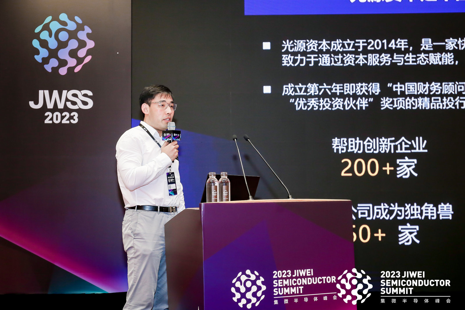
Xu Yinchuan, managing director of Light House Capital (光源资本), said, “China's semiconductor industry is facing the most complicated situation in history. The semiconductor industry chain has bottomed out and is rebounding. In the primary market, it is still at a high level, although the financing scale has dropped slightly in recent years.”
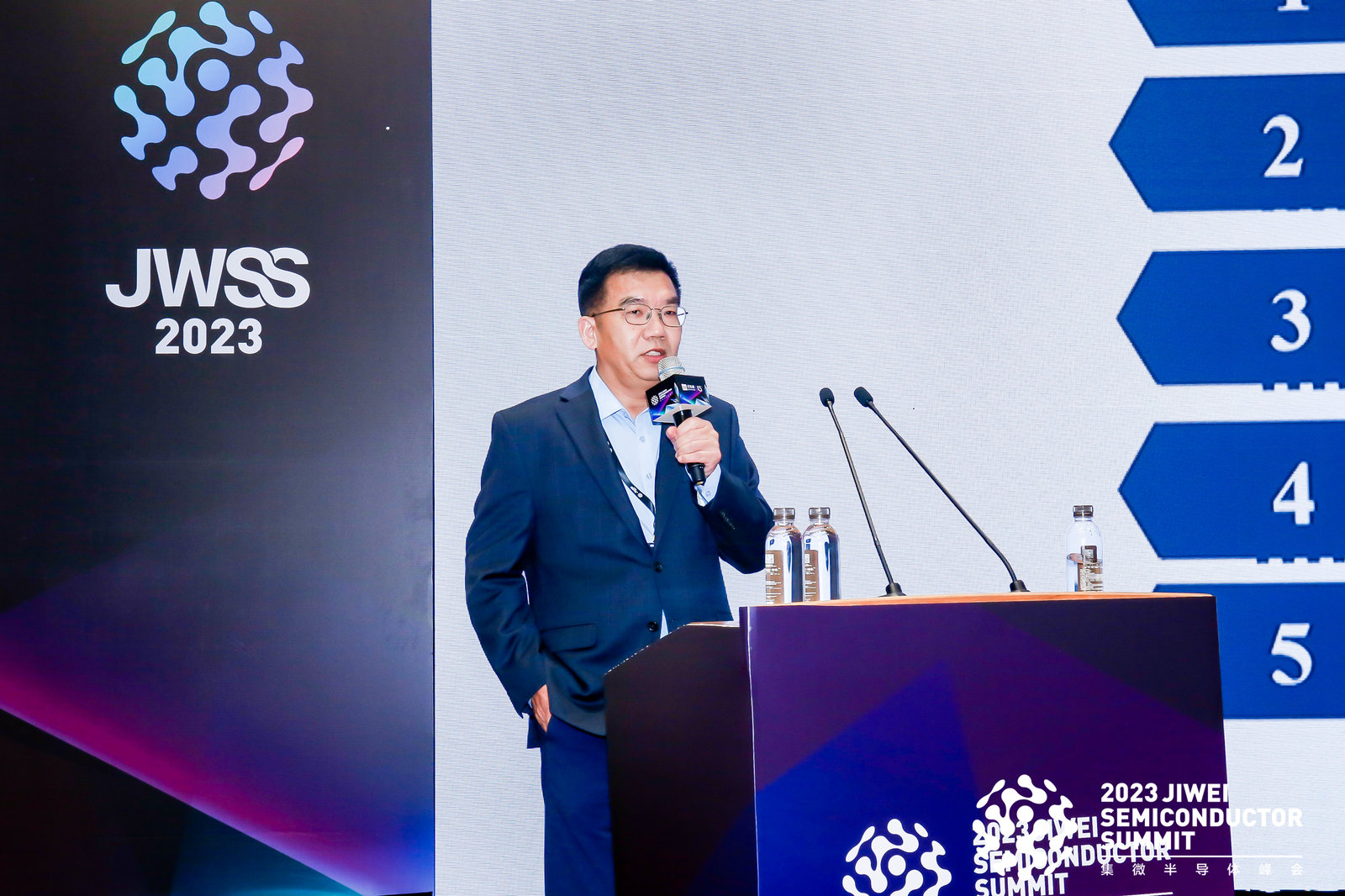
Fan Yonghui, the chief scientist of HatChip (汇芯通信) and WG Tech, said, "With the continuous development of the communication technology industry, new semiconductor materials will be developed towards high frequency, high power, low power consumption, and miniaturization.”
Zhang Zhong, deputy general manager of V-Solution Telecommunication Technology(芯德科技), said, "2.5D/3D packaging technology can improve packaging density. Wafer-level packaging equipment and processes can combine chips with various performances, which can reduce the physical transmission distance to the greatest extent, to achieve the similar function of SOC and be more cost-effective.”
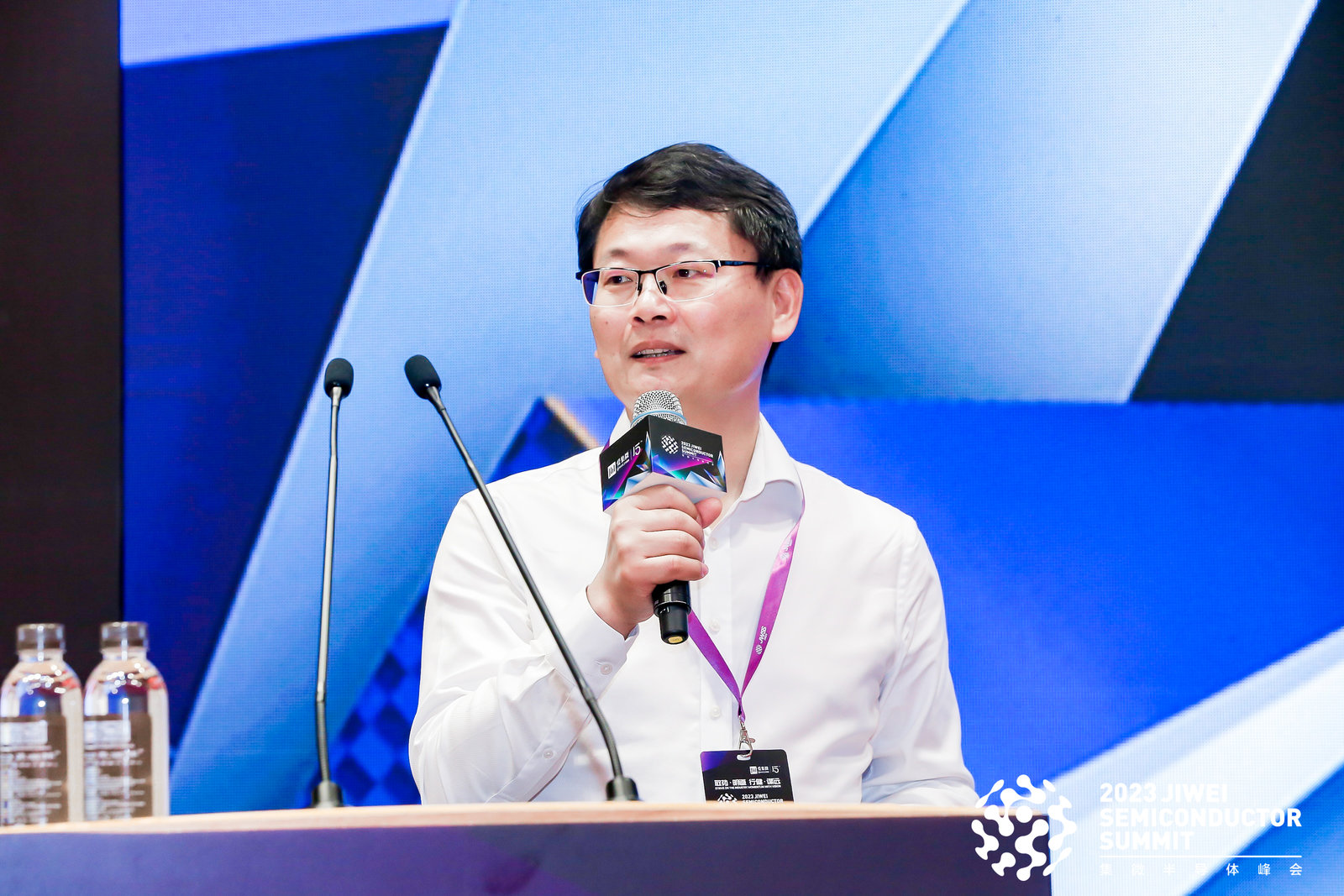
Peng Hongxiu, deputy general manager of Anji Microelectronics, said, “Foreign companies are major players in the wafer wet cleaning market, but Chinese companies have risen gradually and occupied a place. The global electroplating solution market is still dominated by overseas giants, and local solutions are urgently needed to ensure supply chain security.”

Regarding quartz products, Gu Yongming, general manager of YMAT, said, “Chinese manufacturers need to explore high-quality mineral sources, develop quartz purification processes and further reduce the cost of synthetic quartz based on material analysis data. In addition, downstream companies need to give room for trial and error to upstream new material makers.”
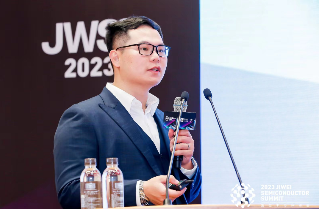
Chen Yuenan, a senior analyst at JW Insights, said, “China’s semiconductor equipment depends on imports. The domestic self-sufficiency rate is only 11% in 2021, judging from equipment purchase data of fabs in China. Those fabs are actively expanding production, opposite to the downward trend of global semiconductor capital expenditures. With more export controls by other countries, the demand for domestic-produced equipment is expected to increase significantly.”
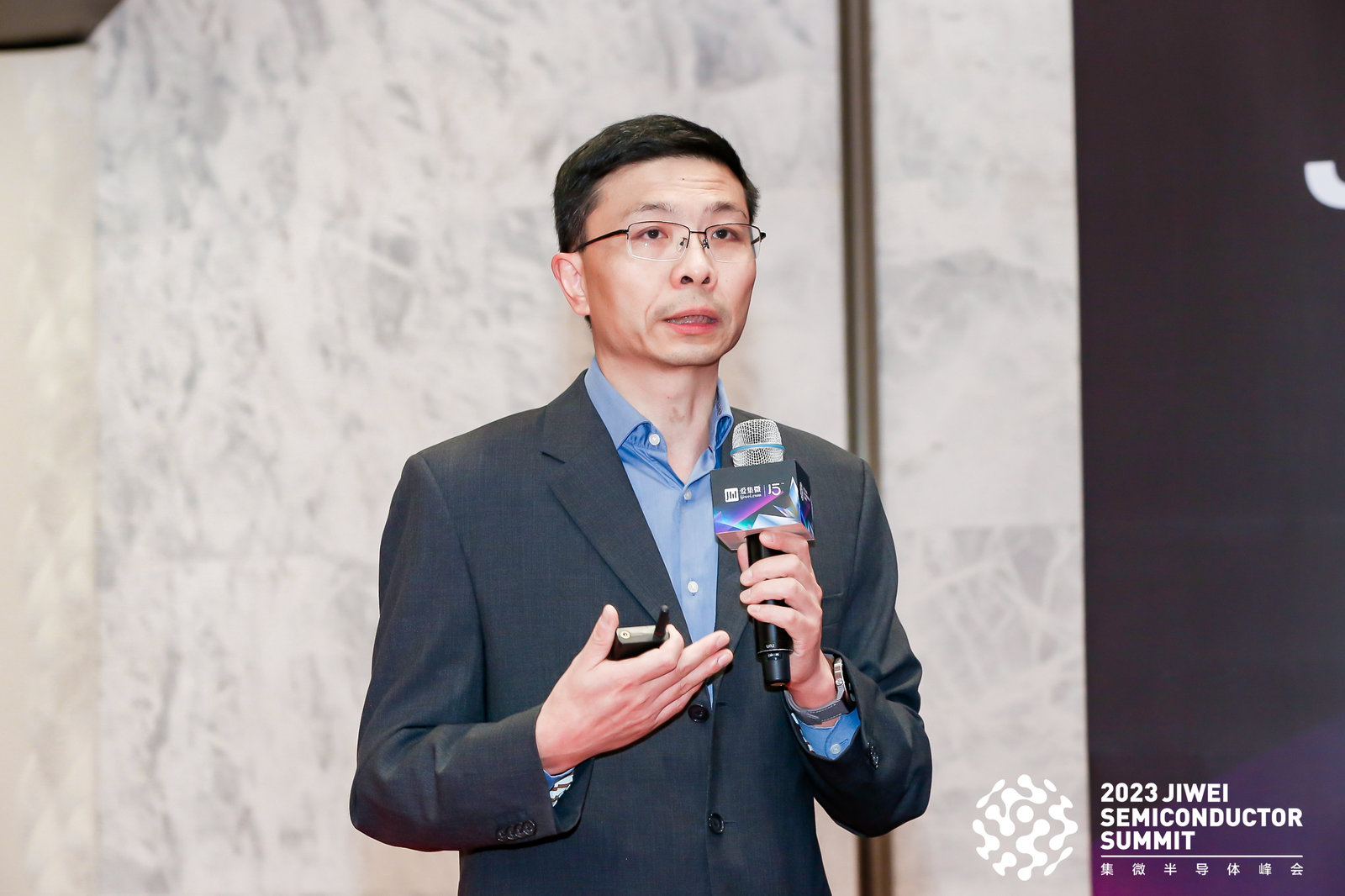
Yang Xiaojun, chairman of SIZONE Technology (众硅科技), said, “The future development of China's IC industry still requires innovative breakthroughs in domestic-produced equipment, which requires collaborative innovation across the entire industry chain.”
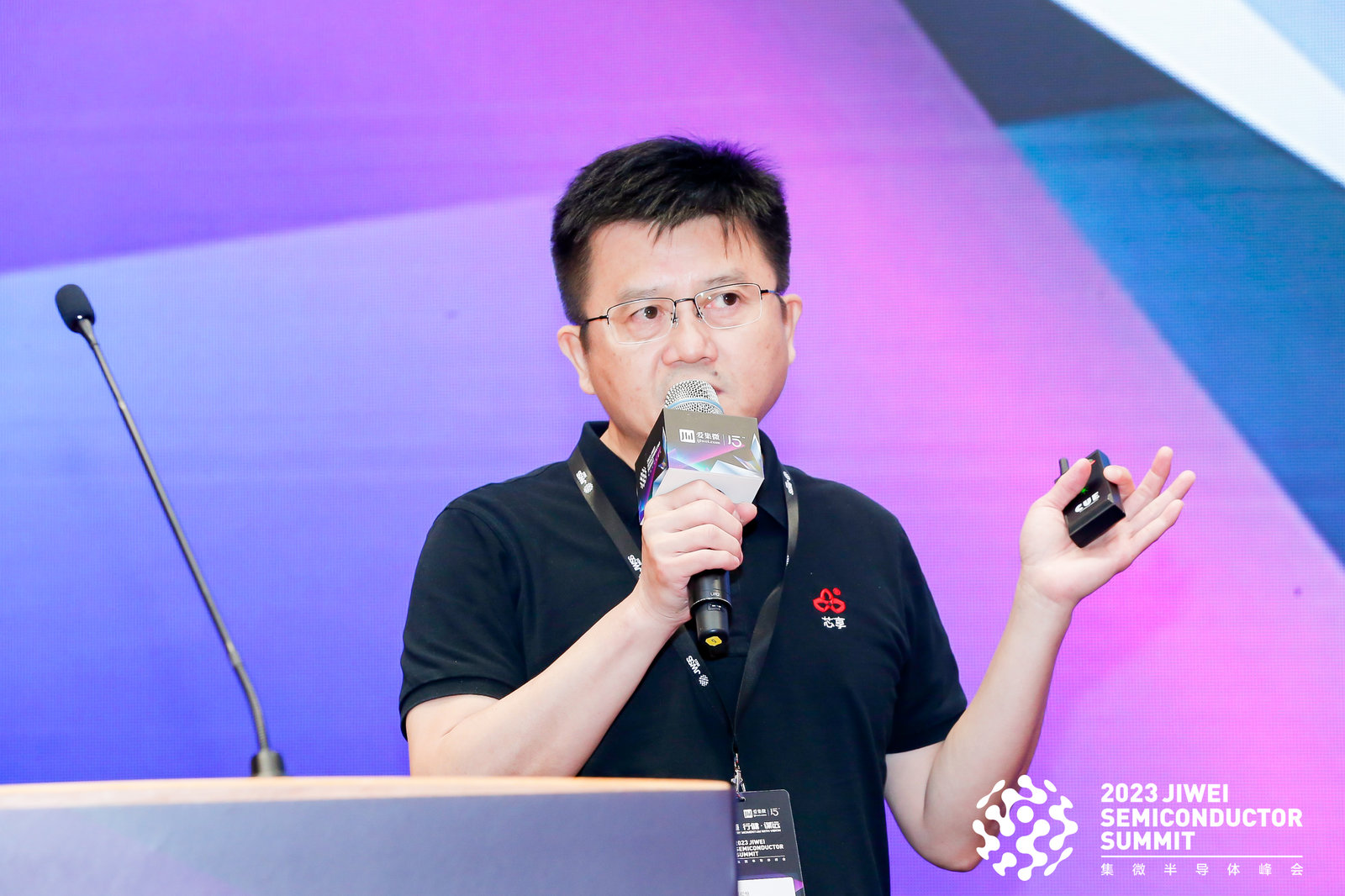
In terms of 12-inch manufacturing equipment, Qiu Songheng, chief marketing officer of Xinxiang Technology (芯享科技), said, “The faster the automation/intelligence capabilities of 12-inch fabs are advanced, the faster the efficiency of fab operation can be improved with shorter production cycle, lower production cost, and higher yield improvement. Therefore, fab manufacturing will be intelligently operated instead of manually.”
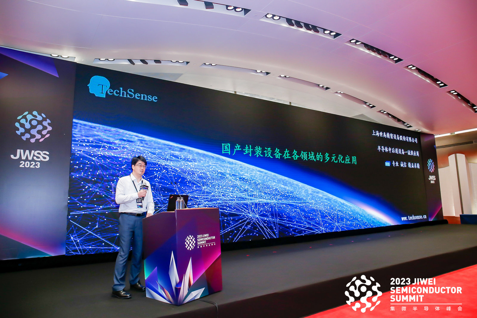
Zhao Kai, general manager of TechSense, said, "Packaging and testing manufacturers require lots of equipment, with some needing to be customized, and the supplier can provide customers with the best solution with its profound technical accumulation and diversified product layout.”
This is the first year for JW Insights to have organized Semiconductor Manufacturing Forum.


